PROCESSOR DESIGN / RTL + SIMULATION ARTIFACTS
A coursework processor built around a shared datapath. The repository has the Verilog modules, per-operation testbenches, waveform setup files, and the course specs.
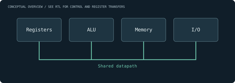
Architecture and scope
The project targets the Cyclone V on the DE0-CV development board, using Intel Quartus and ModelSim. It is a course-specific RISC design, distinct from the separate RV32I planning repository.
The first phase covers registers, a shared bus, and an ALU with arithmetic, logic, shift, and rotate operations. The second adds select-and-encode logic, condition handling, memory, I/O, and instruction scenarios for loads, stores, branches, jumps, and immediate operations.
Design decisions to inspect
- Shared datapath: trace register selection through the bus multiplexer and into arithmetic operations.
- Arithmetic modules: inspect the separate multiply, divide, shift, and rotate implementations.
- Memory interface: follow the RAM and register transfers in the load/store test scenarios.
- Control conditions: inspect branch and jump behavior alongside the condition logic.
Verification artifacts
The repository includes individual testbenches for arithmetic and logic operations in phase_1/demo_files, then instruction-level scenarios in phase_2/demo_files. Waveform scripts in phase_1/waveform_dos support inspection in ModelSim.
These are source and simulation artifacts, not a claim of comprehensive ISA compliance. Published FPGA utilization, timing closure, and measured throughput are not included in this case study.
| Evidence | Location |
|---|---|
| Datapath and arithmetic RTL | CPU source |
| Operation testbenches | Phase 1 demos |
| Memory and instruction scenarios | Phase 2 demos |
| Architecture requirements | CPU specification |